Model-to-Silicon for Physical AI
Chips have always been a rigid part of the stack
Two years to create, and everything northbound must adjust. This spawned way too many layers of human abstraction (CUDA, PyTorch, TensorRT, etc.). Worse, it forced model and application builders to accept the lowest common denominator that a chip provides. Features they don't need and optimizations they can't make.
The old chip design stack was built around human scarcity and walled gardens. RTL, compilers, EDA flows, licensed IP, NDAs, verification boundaries. All of it made sense when humans needed to divide a system too complex to hold in one mind. But AI agents don't need to respect those boundaries.
If you can vibe-code directly in assembly, you don't need a compiler. If you can reliably vibe-code RTL, you don't need the layers above it. The design process itself becomes programmable.
Agents change the space
Agents can reason about model structure, data movement, memory layout, compute topology, scheduling, microarchitecture, and RTL as coupled choices. This turns hardware design into an end-to-end optimization problem: given a workload and constraints, find the best implementation across the software-hardware boundary.
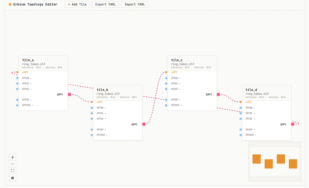
But you can't ask AI to create chip design from scratch. That's an infinite search problem. You need a substrate. A real, open, silicon-proven substrate that agents can reason about, compose, and specialize.
Open software substrate
The substrate has three requirements:
The substrate has to be real.
It must come from hardware that has survived contact with implementation and usage, not from academic exercises that have never been taped out.
The substrate has to be open.
No IP licenses, no NDAs, no worries about foundational LLM CLAs. Agents are welcomed.
The substrate has to be complete.
Tests, simulation, co-simulation, synthesis paths, examples, documentation, and clear contribution flows. Plus real chips, a programmer's manual, a simulator, a runtime, optimized kernels, even a bare metal Go implementation.
AiNEKKO provides this substrate. It lives in AI Foundry and the OpenHW Group of the Eclipse Foundation.
Platforms
AiNEKKO builds composable silicon for edge AI inference. We build across three pillars: RISC-V manycore compute, MRAM-based memory (iRAM), and an open software stack.
New economics
Once design is grounded in a composable substrate, the entire cost structure shifts. Iteration becomes cheap. Exploration becomes parallelizable. Specialization becomes viable at a much smaller scale.
The limiting factor is no longer the cost of committing to a design, but the ability to search through possibilities efficiently. Composability finally gives a boost to product design. AiNEKKO platform building blocks, recomposed for different use cases. Get custom chips without custom tape-outs.
The difference is not incremental. It is structural. It's the difference that can serve the demand of a tape-out every 9 months.
Newsroom
Press coverage, announcements, and industry commentary.
AI Foundry · May 5, 2026
AiNEKKO's manifesto. From model to silicon for edge AI. By Tanya Dadasheva.
Blog
EE Times · 2025
AiNEKKO acquires the hardware IP of Esperanto Technologies, including its manycore RISC-V architecture and toolchain, and open-sources the design under the Eclipse Foundation.
Press
GlobeNewswire · January 29, 2026
AiNEKKO merges with Veevx, combining open RISC-V compute with MRAM-based iRAM technology. Douglas Smith, former Broadcom IP architect, joins the executive team.
Press Release
EE Journal · November 25, 2025
Max Maxfield at EE Journal profiles AiNEKKO. A platform that starts from a proven 1,088-core chip and scales down, not up. A deep dive on open silicon philosophy.
Feature